Our Main research topics
We image in atomic scale
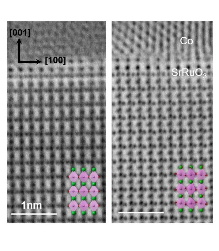
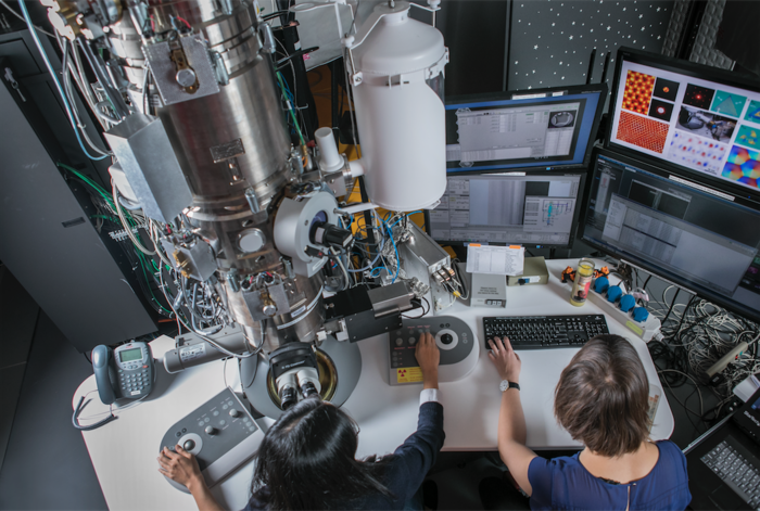
Understanding the physical properties starts from looking the material at an atomic scale with scanning transmission electron microscopy (STEM). Single vacancy or dislocations may sound trivial but it can largely impact the material’s properties.
STEM Analysis
Our research is focused on the following:
Understanding physical phenomena with atomic resolution STEM, looking at interfaces of epitaxially grown films and studying defects
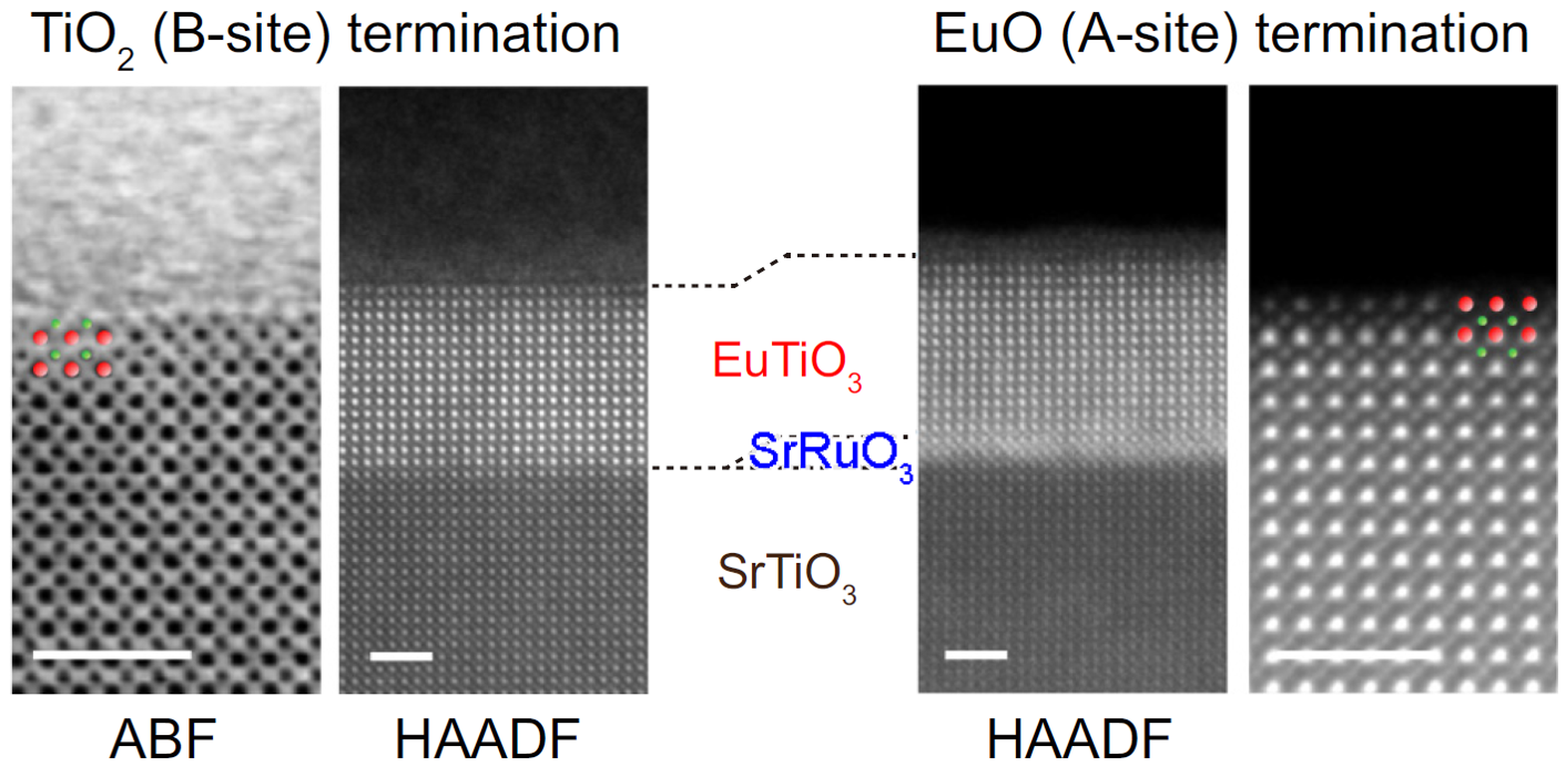
Chemical analysis using EDS or EELS to determine intermixing of composition or surface termination
4D-STEM analysis to obtain phase, strain information
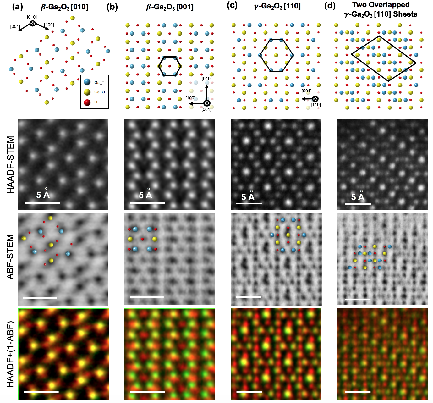
Performs Multislice Electron beam Ptychography (MEP) to understand the dopants, interstitials, interfaces, and the overall 3D structure of the system with the best resolution.
Why is this important?
Some physical phenomena can only be understood by looking at atomic resolution, such as nano-domains, chemical intermixing, and phase formation inside the material.
Defects, dislocations, and strain can largely affect the materials properties and also device performance.
MEP can achieve the world-record resolution of 23 pm, enabling access to more information
Current Projects:
Identifying the phase of nano-domains in Hf-based oxide films
Surface termination study related to ARPES
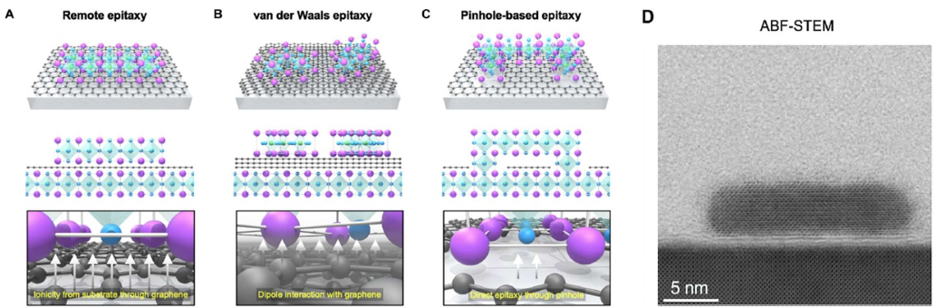
Identifying atomic registry for remote epitaxy and freestanding membranes
Atomic-res chemical analysis before and after chemical reaction
Ongoing Samsung project on strain mapping of devices using MEP
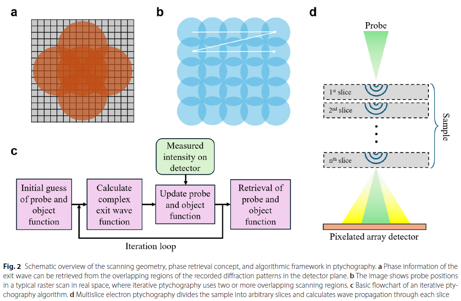
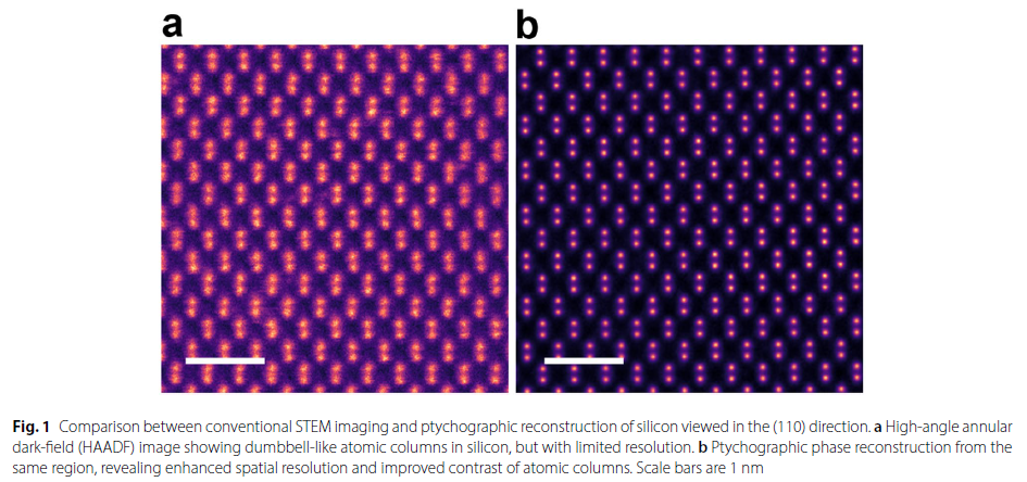
Electron beam ptychography
We grow and deposit materials
We use Pulsed laser deposition (PLD) to grow various complex oxide thin films. Currently we are focusing on high-k dielectric epitaxial films.
Our research is focused on the following:
Utilizes pulsed laser deposition (PLD) to grow high-k oxide films epitaxially
Fabrication of all-oxide transistors having a clean interface
Manipulating materials properties through composition control
Why is this important?
By performing epitaxy, we can do strain engineering - utilizing the lattice parameter differences between the substrate and the film, one can control the physical properties through strain - leading to favorable phase transition or enhanced polarization
Device performance is largely affected by heterogeneous interfaces, where 2DEG formation as well as leakage current can occur. Thus it is crucial to create a chemically sharp interface
Through multiple target deposition we can control subtle composition tailored to our needs.
Current Projects:
High-k oxide films with low leakage current enabled by composition control
Low temperature growth of oxides for future devices
Manipulation of polarization and coercive field by composition control
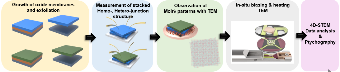
We make freestanding films
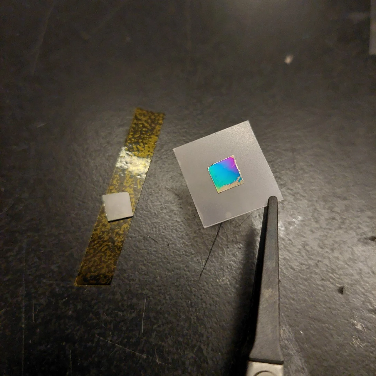
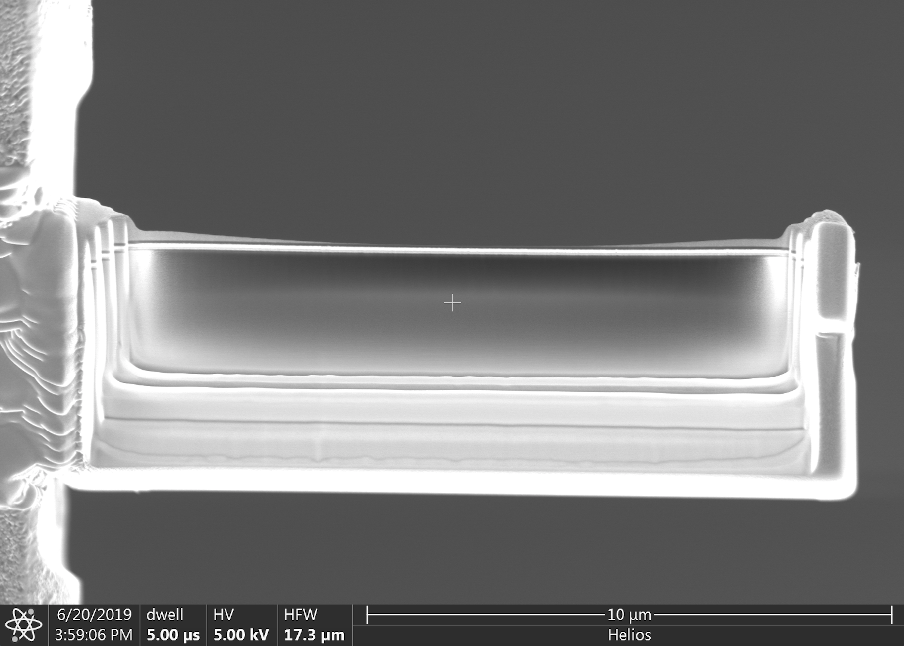
We use water soluble sacrificial layer, and buffer-free exfoliation to make freestanding oxide thin films with thicknesses ranging from few nms to several hundreds of nanometers. These can later be integrated into flexible, light-weight devices.
Our research is focused on the following:
Methodology of obtaining freestanding oxide films
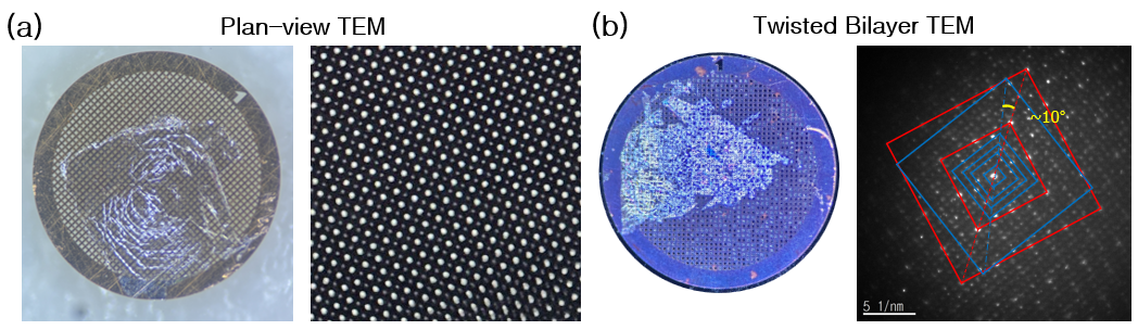
Integration and physical coupling of freestanding membranes
Basic study of freestanding membranes before and after exfoliation
Why is this important?
Freestanding oxide membranes eliminate substrate clamping, enabling strain-free behavior or controlled strain engineering, and thus revealing intrinsic electronic, magnetic, and ferroic properties
Their transferability allows stacking, bending, and integration into unconventional architectures, enabling novel interface physics and curvature-driven effects, as well as making them suitable for flexible electronics and heterogeneous integration
Current Projects:
Exfoliation of High-k oxide films
Basic defect propagation study in freestanding membranes using MEP
Device fabrication using oxide freestanding membranes